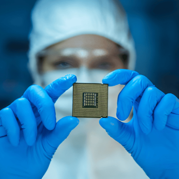
Trusted Partner in Semiconductor Innovation
Accelerating Chip Design from Concept to Silicon
Neetha Consulting LLC delivers high-performance VLSI and semiconductor design services tailored for next-generation technologies. With deep expertise across ASIC, FPGA, SoC, and physical design, we help global companies bring their ideas to life – faster, smarter, and more efficiently.
What We Do
We help companies design the chips that power the world.





What Makes Us Unique
Silicon-Proven Expertise
We’ve delivered over 30 successful tapeouts across leading technology nodes.
End-to-End Design Capability
From architecture to tapeout, we handle the complete chip design cycle.
Global Engineering Talent
Our 150+ engineers across four countries bring global insight to every project.
High-Speed Design Experience
We’ve designed processors running at speeds up to 6.6GHz with precision.
Flexible Engagement Models
Choose from turnkey delivery, ODCs, or talent augmentation based on your need.
Fast Turnaround, Zero Compromise
We’re known for solving last-mile timing and signoff issues under tight deadlines.
Deep Domain Knowledge
Specialized in RF, AI/ML, IoT, and telecom chip solutions.
Custom Methodologies
We build scalable design frameworks tailored for startups and large teams alike.
Leadership with 30+ Years of Vision
Guided by a seasoned chip lead with a legacy of 200+ global tapeouts.
Why Choose Neetha Consulting LLC?
- Reliable
- Specialized
- Scalable
Projects Successfully
Satisfied Clients
Skilled Engineers Across the Globe
Successful Tapeouts Delivered
Years of Semiconductor Excellence
Global Engineering Hubs
About Neetha Consulting
Powering Innovation in Chip Design Since 2007
With 150+ engineers and 16+ years of expertise, we help global clients bring complex semiconductor ideas to life—faster, smarter, and more efficiently.
Our industry
Discover our deep expertise in your industry








Our Testimonials
What Our Clients Say
Rajesh Menon
VP Engineering
“Neetha’s team handled our complex SoC integration with unmatched precision. Their deep technical know-how and timely delivery helped us hit a critical product launch window.”
5.0 RATING
Anita Desai
Design Lead
“From RTL design to final tapeout, Neetha Consulting was a true partner. Their engineering talent and flexibility made them an extension of our in-house team.”
5.0 RATING
Michael Lee
CTO of Global Retail Hub
“The physical design support we received was top-tier. Their expertise in timing closure and DRC clean layouts gave us confidence, even under tight schedules.”
5.0 RATING
Suresh Patil
COO of SmartLogix
“What stands out about Neetha is not just their technical skills, but their proactive communication and solution-oriented approach.”
5.0 RATING
Brian
Managing Director
“From RTL to GDSII, Neetha handled our entire SoC design with absolute professionalism. They’re more than a vendor—they’re our design partner.”
5.0 RATING
Frequently Asked Questions
Got Questions?
Explore some of the most common questions our clients ask about our services, team, and capabilities.
We specialize in end-to-end chip design services including ASIC & FPGA design, SoC architecture, physical layout, and EDA tool expertise.
Our global presence includes offices in Cupertino (USA), Hyderabad (India), Dhaka (Bangladesh), and Penang (Malaysia).
Yes, we offer complete turnkey solutions from specifications to tapeout, including verification, layout, and design closure.
Absolutely. We offer custom engagement models and methodology development tailored for early-stage semiconductor startups.
We serve a variety of industries including consumer electronics, automotive, healthcare tech, telecommunications, and defense.
Get In Touch
We have a strong global presence, marking our commitment to delivering tech excellence in key markets worldwide.

Cupertino, USA
hr@neethaconsulting.com
Neetha Consulting LLC 10080 North Wolfe Road, Suite SW3-200 Cupertino, CA 95014 📞 (408) 368 7120.

Hyderabad, India
Our Hyderabad office serves as a major engineering hub focused on ASIC/FPGA design, SoC development, and design verification for global projects.

Dhaka, Bangladesh
The Dhaka center specializes in backend design, IC layout, and manufacturing support, contributing to seamless production and tapeout readiness.

Penang, Malaysia
Strategically positioned in Southeast Asia’s tech corridor, our Penang team leads design automation, QA, and testing services for complex silicon systems.